- 您现在的位置:买卖IC网 > Sheet目录338 > LV8498CT-TE-L-H (ON Semiconductor)IC MOTOR DRIVER S111 WLP
LV8498CT
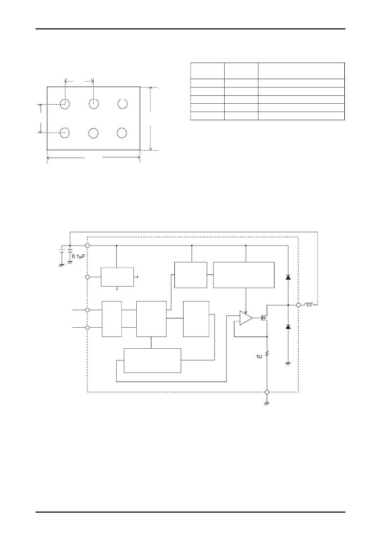
Pin Assignment
Bottom View ( Ball side up )
3
2
1
Pin No.
Pin Name
Pin Description
A1
SCL
I 2 C SCL input pin
0.4
A
A2
A3
B1
B2
ENA
GND
SDA
VCC
Enable & reset *1, 2
Ground
I 2 C SDA input pin
Power supply pin
0.4
0.87
B3
OUT
Output pin
B
*1 : Setting the ENA pin to low powers down and resets the IC.
1.27
It is necessary to power on the IC by setting the ENA pin to
low and hold it high during normal operation.
*2 : When the ENA pin is to be used with pull_up, it is necessary to
send code 0 in advance after power-on.
Block Diagram
VCC
ENA
Bias
ON/OFF
Reference
voltage
Voltage drop protection
&
thermal protection
RESET
VCM
SDA
DAC
SCL
I 2 C
IF
I 2 C
DECODE
10bit
current
+
-
OUT
setting
RF
Timing genaration
GND
No.A1625-3/8
发布紧急采购,3分钟左右您将得到回复。
相关PDF资料
LXC100-4200SW
POWER SUPPLY LED 100W 4200MA
LXC120-4900SW
POWER SUPPLY LED 120W 4900MA
LXC150-5950SW
POWER SUPPLY LED 150W 5950MA
LXC25-2080SW
POWER SUPPLY LED 25W 2080MA
LXC35-2900SW
POWER SUPPLY LED 35W 2900MA
LXC40-3330SW
POWER SUPPLY LED 40W 3330MA
LXC50-4200S
POWER SUPPLY LED 50W 4200MA
LXC60-5000SW
POWER SUPPLY LED 60W 5000MA
相关代理商/技术参数
LV8548M
制造商:未知厂家 制造商全称:未知厂家 功能描述:
LV8548MC
制造商:SANYO 制造商全称:Sanyo Semicon Device 功能描述:Bi-CMOS integrated circuit 12V Low Saturation Voltage Drive Forward/Reverse Motor Driver
LV8548MC-AH
功能描述:马达/运动/点火控制器和驱动器 2-CH BRUSH MOTOR DRIVER
RoHS:否 制造商:STMicroelectronics 产品:Stepper Motor Controllers / Drivers 类型:2 Phase Stepper Motor Driver 工作电源电压:8 V to 45 V 电源电流:0.5 mA 工作温度:- 25 C to + 125 C 安装风格:SMD/SMT 封装 / 箱体:HTSSOP-28 封装:Tube
LV8548MC-BH
功能描述:马达/运动/点火控制器和驱动器 GP DC MOTOR DRIVER
RoHS:否 制造商:STMicroelectronics 产品:Stepper Motor Controllers / Drivers 类型:2 Phase Stepper Motor Driver 工作电源电压:8 V to 45 V 电源电流:0.5 mA 工作温度:- 25 C to + 125 C 安装风格:SMD/SMT 封装 / 箱体:HTSSOP-28 封装:Tube
LV8548MCZ-AH
制造商:ON Semiconductor 功能描述:2-CH BRUSH MOTOR DRIVER - Tape and Reel 制造商:ON Semiconductor 功能描述:Motor / Motion / Ignition Controllers & Drivers 2-CH BRUSH MOTOR DVR 制造商:ON Semiconductor 功能描述:REEL / 2-CH BRUSH MOTOR DRIVER
LV8548MGEVB
功能描述:电源管理IC开发工具 EVM FOR LV8548M
RoHS:否 制造商:Maxim Integrated 产品:Evaluation Kits 类型:Battery Management 工具用于评估:MAX17710GB 输入电压: 输出电压:1.8 V
LV8548M-TLM-H
功能描述:马达/运动/点火控制器和驱动器 4-16V SteppingMotor 2chBrush Motor Dr
RoHS:否 制造商:STMicroelectronics 产品:Stepper Motor Controllers / Drivers 类型:2 Phase Stepper Motor Driver 工作电源电压:8 V to 45 V 电源电流:0.5 mA 工作温度:- 25 C to + 125 C 安装风格:SMD/SMT 封装 / 箱体:HTSSOP-28 封装:Tube
LV8548M电机驱动
制造商:未知厂家 制造商全称:未知厂家 功能描述:
